Provide a project file in CAM350 or Gerber formats.
Provide a multiplied billet file in CAM350 or Gerber formats (if boards are in the billet).
Provide an assembly drawing or assembly diagram containing:
- cross sections;
- sections and dimensions;
- position designations of components and their orientation (polarity designation must be unambiguous and correspond to the real appearance (point, bevel, protrusion, etc.));
- technical requirements for installation and mounting of components;
- component installation options;
- footnotes for non-standard component installation.
Provide a specification-list of components indicating:
- component name;
- rating;
- housing type;
- position designation;
- quantity.
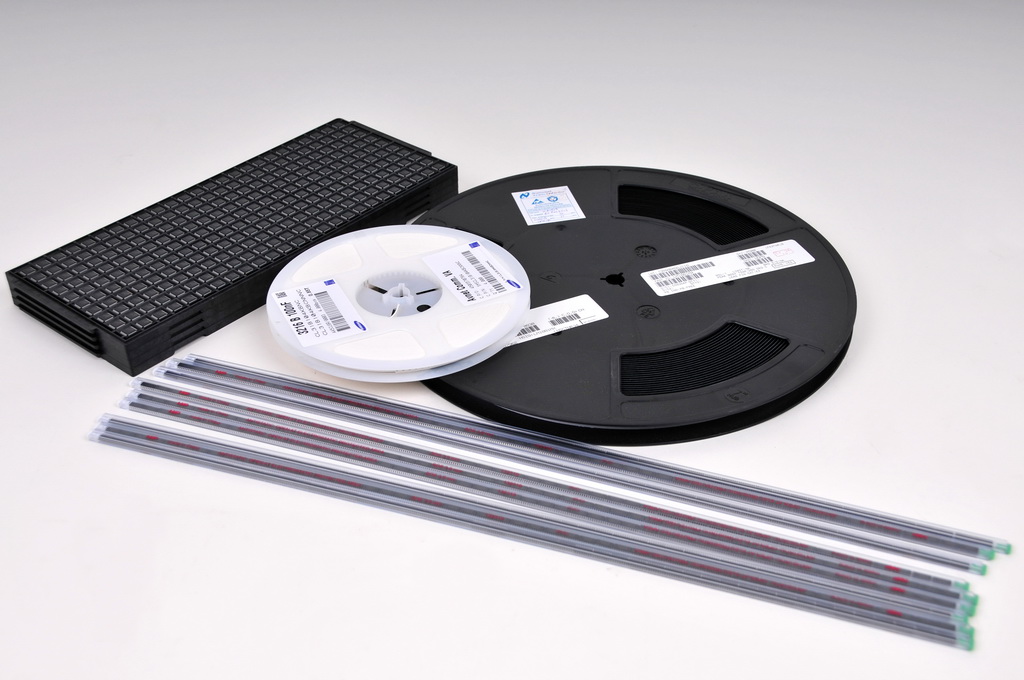
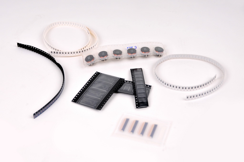
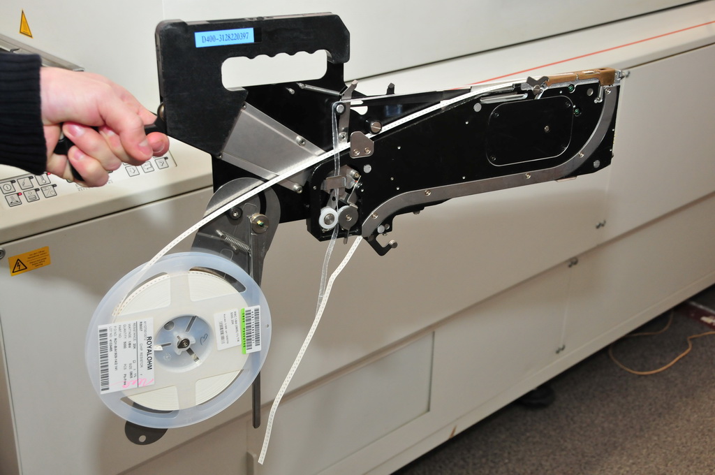
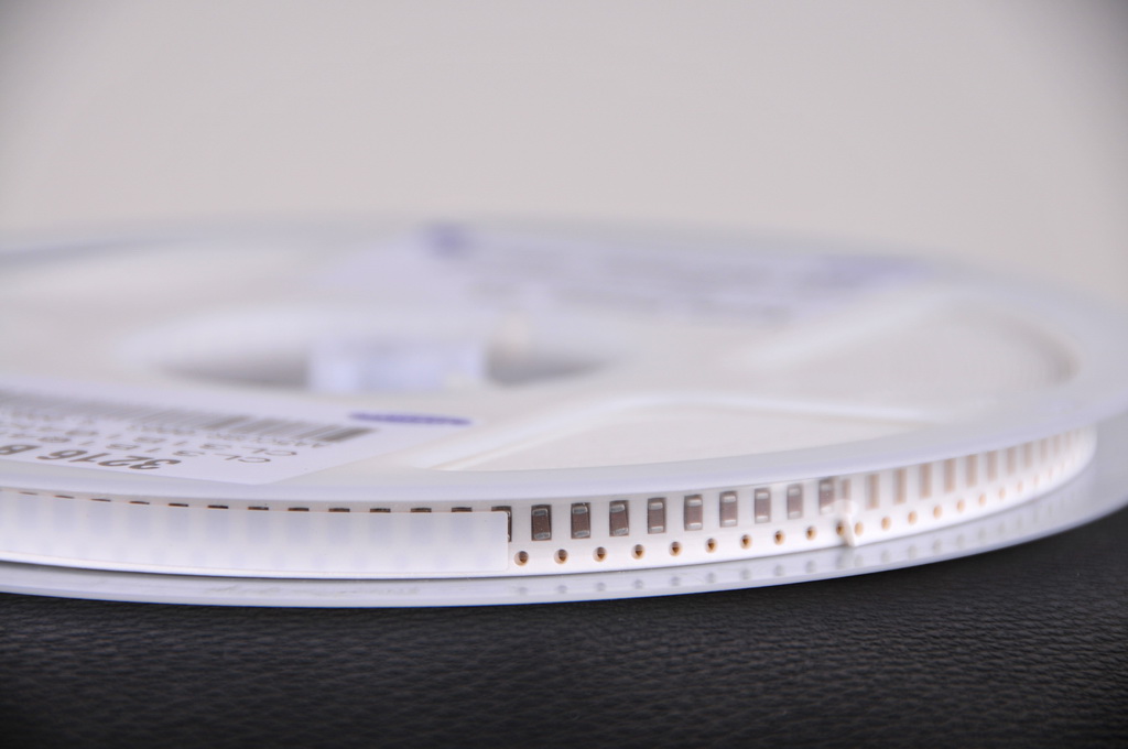
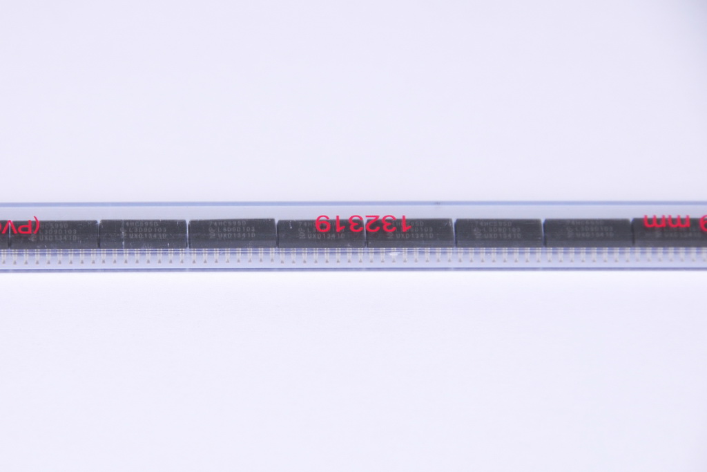
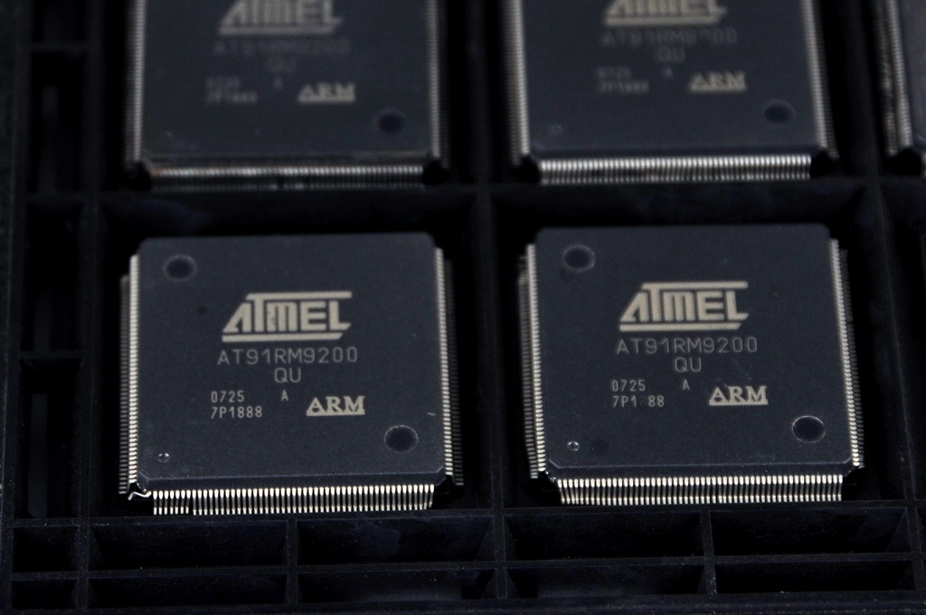
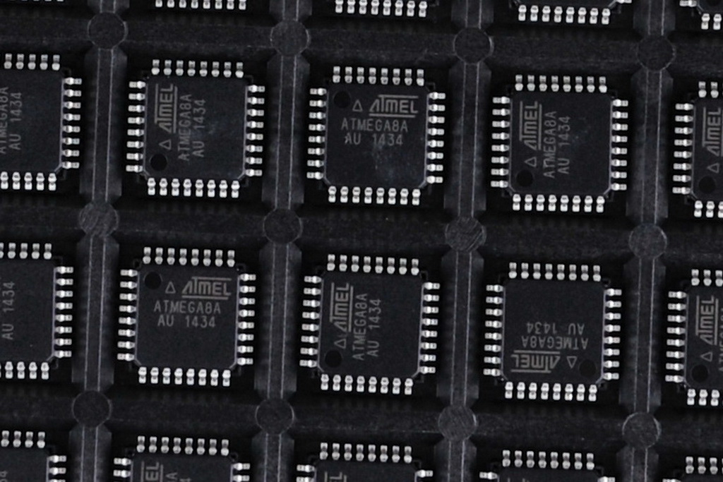
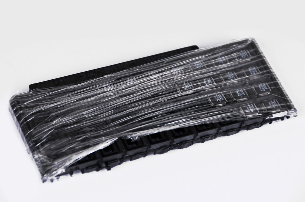
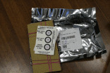
We accept components in the following types of media: coils (8, 12, 16, 24, 32 and 44mm) pouches of any width, matrix trays for microchips.
SMD components should be delivered with a reserve of at least 2%.
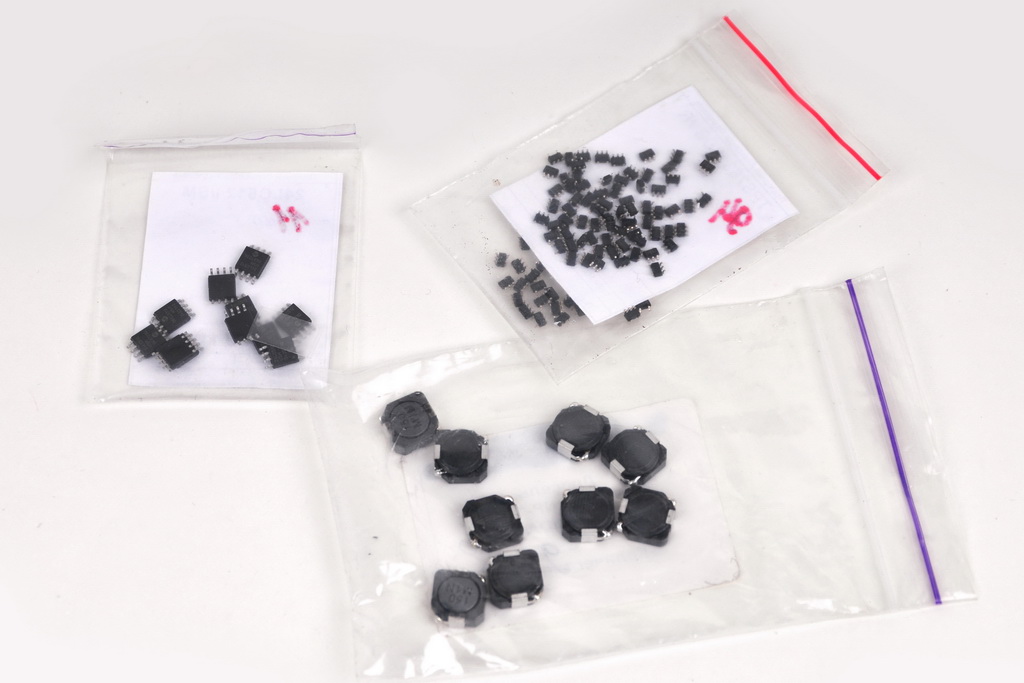
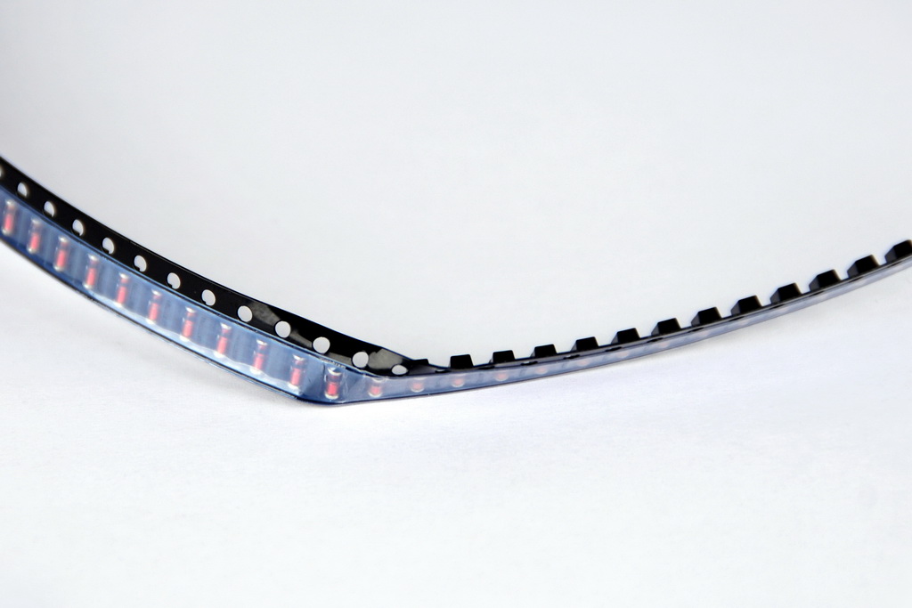
Such defects are unacceptable:
- deformation of component pins;
- deformation of tape with components;
- violation of vacuum packaging;
- detachment of protective film.
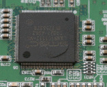
Component placement
Components should preferably be placed on the same side of the board. If this condition cannot be met, divide the components into “light” and “heavy” and place them on different sides of the board. Tall components (over 8mm) should also be placed on the “heavy” side.
Single and double-sided boards
For surface mounting, PCBs with SMD (Surface Mount Device) elements on one side are much more technologically advanced. The assembly of a single-sided PCB is much faster than a double-sided PCB, as there is no need to rebuild the machine from one side to the other. For a double-sided PCB, programmes are written twice on the equipment, the equipment is reconfigured twice, two stencils are made, etc. This should be done only if the dimensions of the board itself, all sorts of restrictions on clearances between conductors, contact pads and other elements of the board, and other requirements leave no choice. It should be remembered that, firstly, the cost of mounting each side of the board is calculated as for a separate product, and, secondly, for the installation of double-sided printed circuit boards there is a coefficient of markup. And this applies to the vast majority of mounting companies. In addition, the cost of test equipment to check the PCBs themselves increases significantly.
Components should be positioned no closer than 1 mm from the edge of the workpiece if there are process margins and 5 mm if there are no process margins.
Gaps between components:
- 0.3 mm – minimum possible gap;
- 0.4…0.5 mm – between chip components;
- 1 mm – between chip components and large components of the board;
- 1 mm – between chips and large components;
- 1 mm – between SMD and lead components.
For components with pin pitch of 0.5 mm and less, if possible, leave space (on the diagonal of the component) for local reference marks.
Orientation of components
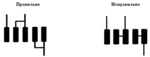
Components with polarity should preferably be orientated in the same way.
Component sizes
It is desirable that as many components as possible have the same housing size. For example: resistors and capacitors – 0805.
The maximum height of a component must not exceed 15 mm.
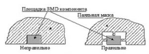
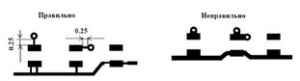
Connection of conductors to SMT pads
The contact pads of components must be separated with solder mask from transition holes, contact pads, etc. Connect contact pads and wide conductors with a narrow conductor. The width of the supply “narrow” conductor should be selected depending on the accuracy class of the board and the current flowing through it.

All jumpers between the legs of SMT components must be outside the soldering area.
SMD component areas located on large polygons should be separated from the polygon by jumpers (thermal barrier), except when the polygon is used as a heat sink.
Transition holes
Do not locate transition holes on the component’s contact pads.
Marking
Markings on the board are made in the conductor layer or by silkscreening (silkscreened markings should preferably be placed only in the areas of the board covered by a protective mask).
Graphical and position designations of components should reflect polarity and orientation of components on the board.
Marking elements of components located next to each other must not overlap and overlap (marking elements falling on the areas open from the mask and covered with the finish coating will not be applied).
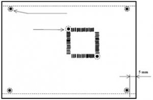
Reference marks
A minimum of two global marks (reference marks) are required, usually located at diagonally opposite corners of the board as far apart as possible but no more than _400_mm. Global marks should be on all layers containing components.
In this case, if the length of the board is more than 400 mm, asymmetrical arrangement of reference marks is allowed – one at a distance of no more than 5 mm from the edge of the board, the other at a distance of no more than 400 mm from the first.
Local reference marks are usually placed diagonally around the perimeter of the area occupied by the component. In case of lack of free space, it is allowed to use one local reference mark preferably in the centre of the area occupied by the component
Reference marks should preferably be in the form of a painted circle with a diameter of 1 mm (all reference marks should be of the same shape and size).
There must be a restricted area around the markings for conductors, components and the protective mask.
There must be a distance of at least 5mm plus the width of the restricted area between the marks and the edge of the board.
All tags must be imaged in the conductor layer.
Tags must be unmasked and have a smooth, highly light reflective, metallic coating (nickel, tin alloys, silver,…).
All tags shall be located outside the prohibited areas for conductors and components.
Board blanks
The deformation of the board blank must not exceed (0.5 mm + board thickness).
It is desirable that the blank is rectangular in shape. This is necessary for its clear fixation on the assembly table. However, the production of blanks with more complex shapes is not excluded.
Polygons on the outer and inner layers (for multilayer boards) should be placed evenly on the surface of the board and made in the form of a grid of conductors (to prevent deformation of the board).
Conductors and transition holes placed under BGA packages must be covered with a protective mask.
The distance from the edge of a non-metallised hole to a contact pad or conductor must be at least 0.5 mm.
Workpiece parameters:
- recommended workpiece size 200×300 mm
- thickness of the board blank sheet 0.5…4.2 mm
- maximum mass of the PCB blank 3 kg
If necessary, single boards are combined into a panel.
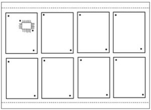
The board spacing must be in accordance with the requirements of the applied board separation technology:
- milling
- scribing
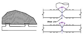
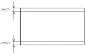
Technological zones
The process zones are usually located along the long side of the workpiece and have a width of 5 mm. Technology zones are separated from the workpiece by scribing or bridging. (If the use of process zones is unacceptable, component-free areas must be provided on the board that conform to the characteristics of the process zones).
For quality and fast solder paste application it is recommended to choose stencils made of polished stainless steel rather than bronze or polymer. Bronze, as a softer material when the stencil is stretched, causes deformation of the apertures in the stencil, which can lead to displacement of the solder paste pattern and subsequent formation of jumpers between component pins or residual solder balls on the PCB surface of the assembled electronic assembly.
Requirements for stainless steel stencils
The maximum working area for a steel stencil should be 510×510 mm.
If the PCB has components with a pitch of 0.5 mm or less, it is better to use a stencil made of 0.1 mm thick material, if not, it is better to leave 0.127 mm. For mounting components with smaller pitches (including microBGAs), it is necessary to use 0.08mm thick material.

DOWNLOAD GERBER STENCIL FRAME FILE
Requirements for bronze and polymer stencils
The recommended size of stencils should not exceed 400×250 mm, but it is possible to use stencils up to 400×900 mm. The material thickness for bronze stencils should be selected in the same way as for steel stencils.

If a bronze or polymer stencil is used, process margins of at least 100 mm in length, and 20 mm in width from the outermost components must be provided.